Ensuring Airborne Molecular Contamination (AMC) Control
In semiconductor / clean manufacturing environments, two aspects of molecular contamination control need to be understood: (1) the background levels of contamination existing under stable conditions, and (2) the elevated concentrations that occur during contamination events.
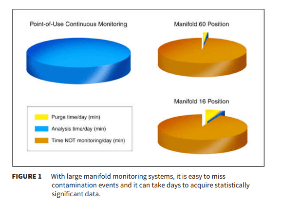
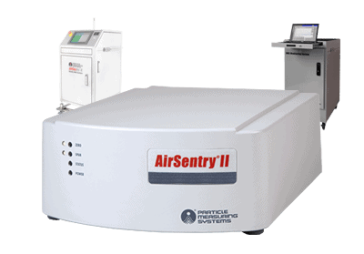 A new approach to monitoring both aspects of molecular contamination control is presented. Recent technical advances have made it feasible to perform continuous, real-time monitoring of critical locations in clean manufacturing environments with significant advances in sensitivity and stability. These improvements are realized by using a small, low-cost monitor that is dedicated to continuously monitoring a single, critical location.
Additionally, a distinction needs to be made between critical and non-critical environments. Critical locations are those where either processes or products are directly at risk for damage from molecular contamination or where a known potential contamination source exists. Non-critical contamination areas are typically cleanroom environmental monitoring and return air monitoring. Contamination levels in these areas do not have as direct of an impact on products and processes, but are indicative of general cleanliness. Optimal monitoring solutions for critical and non-critical locations need to be implemented as part of a complete facility monitoring system.
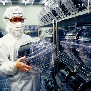
Yield losses due to molecular contamination issues started to emerge in semiconductor manufacturing almost 30 years ago. At this time, contamination monitoring was typically conducted by manually by pulling air samples through a bubbler or impinger. Then, the samples would be taken to a chemical analysis laboratory to determine the content. This process is very labor intensive and it can take days to obtain a result. Samples were usually collected as a reactive measure to determine the cause of yield problems or as part of monthly or quarterly monitoring program.
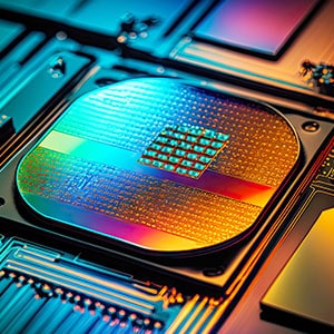
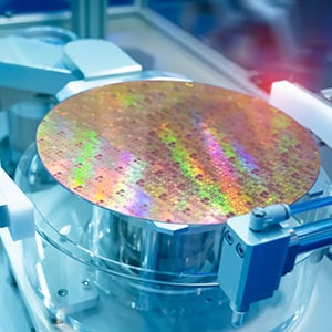
As semiconductor manufacturing has progressed to 90 nm node and beyond in the last decade, increasingly cleaner environments have been required, especially for 193 nm photolithography. This has resulted in an emerging need for continuous monitoring in critical locations and improved monitoring strategies for noncritical locations.
Complete the form to get the complete paper.
Get a solution for your Airborne Contamination Monitoring needs.